

用水大户台积电为何在美国缺水地区建厂?
DYLAN SLOAN
2024-04-10
中国台湾半导体厂商台积电获得美国商务部66亿美元补贴,在凤凰城新建三座晶圆厂。
 文本设置
文本设置
 Plus(0条)

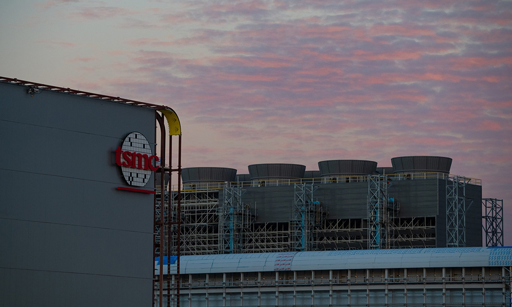
美国商务部周一宣布,将向中国台湾半导体厂商台积电(TSMC)拨款66亿美元。除了目前正在施工的两座工厂外,台积电将在亚利桑那州新建第三座芯片工厂。这笔拨款将是拜登政府将不可或缺且具有重要战略意义的计算机芯片供应链重新引回美国的重要举措。
但在新厂所在的凤凰城,台积电却面临一个悬而未决的难题:作为美国最缺水的城市之一,凤凰城如何满足工厂的用水需求?
半导体生产要消耗大量水资源。标普全球评级(S&P Global Ratings)的一份报告显示,全球半导体产业的耗水量几乎与整个纽约市的用水量相当。这份报告认为供水问题是半导体发展面临的潜在威胁。
标普在2月警告称:“我们认为,未来十年,缺水将是科技硬件产业面临的一大风险,尤其是用水密集型半导体领域。如果不能妥善应对这个风险,可能影响芯片厂商的运营和信用。”
凤凰城已经经历了十多年的干旱。事实上,去年,由于地下水不足,亚利桑那州对部分新房开发项目施加了限制。但当地官员表示,随着该地区崛起成为美国重要的芯片中心,凤凰城可以满足台积电甚至更多公司的用水需求。
凤凰城水资源管理顾问辛西娅·坎贝尔对《财富》杂志表示:“对于水这种有限的、宝贵的资源,如果一家[工厂]会消耗大量水资源,这就会涉及经济上的权衡。我们确实[有足够的水资源]。”
半导体晶圆厂需用水冲洗微小硅片,计算机芯片就是在这些硅片上制造而成。随着ARM和英伟达(Nvidia)等设计公司开发出更复杂的新一代尖端芯片,以支持人工智能等技术,台积电生产芯片的用水量增多。尽管台积电也采取了水资源重复使用的策略,并计划达到90%的循环利用率,但近几年其单位用水量持续增多。
依旧有一些专家质疑台积电的策略可能产生的实际效益。
纽芬兰与拉布拉多纪念大学(Memorial University of Newfoundland and Labrador)的教授、电子产业资源利用与浪费领域的专家约什·莱帕夫斯基表示:“90%的循环利用率听起来不错。但这意味着有10%的水被浪费或没有被循环利用,这是显而易见的。每十天就需要100%更换一批‘新的供水’。”
除了用水以外,芯片工厂还会产生废水,因为芯片生产使用的化学品,会产生有害的或未知的环境影响。去年8月,一个半导体制造商联盟反对美国环境保护署禁止使用全氟烷基和多氟烷基物质(PFAS)的拟定法规,他们认为该项法规会导致半导体制造商无法在美国生产设备,并警告“环境保护署如此草率的行动,会造成难以估量的经济后果”。PFAS是一种“永久性化学品”。
从2018年到2022年,台积电的废水排放量减少了30%,且公司承诺其在亚利桑那州的三座晶圆厂将实现“近零”废水排放率。但这同样遭到了质疑。
莱帕夫斯基称:“近零废水排放……没有一个具体的数字。是0.1,还是1?或者是10?”
凤凰城的坎贝尔表示,该市的水务官员尚不确定台积电的具体废水排放率,但当局已经在与该公司密切沟通其用水和水处理计划。台积电和美国商务部均未立即回应置评请求。
台积电预计三座晶圆厂要到2028年才会投入生产,并且可能服役数十年。莱帕夫斯基表示,在此期间,凤凰城的供水情况可能会恶化。但台积电已经投资了650亿美元,再加上联邦政府的拨款,对台积电而言,搬到更绿色的草原(按照字面意义理解)将是难以接受的。
莱帕夫斯基表示:“这些工厂应该要持续生产10年、20年甚至30年。这是应对气候变化的期限。如果你投入了数十亿美元建设这种量级的……新工厂,当供水状况恶化到构成问题的程度,你不可能只是把它搬到其他地方。”
对于供水不足会是台积电面临的重大挑战这种说法,亚利桑那州的其他官员也进行了反驳。去年8月,亚利桑那州工商业联合会(Arizona Chamber of Commerce and Industry)CEO丹尼·塞登在一篇专栏文章中写道,亚利桑那州通过提高用水效率和节约用水,能够满足用水需求。他提到台积电的竞争对手英特尔(Intel)在亚利桑那州钱德勒的工厂,该工厂通过现场回收设施,每天可处理900多万加仑水。
随着亚利桑那州继续打造半导体制造中心,坎贝尔表示,凤凰城的供水将足以满足更多项目的需求,只要这些项目符合预期。
他预测道:“水资源并非无穷无尽的,在某个时间点会达到极限。但根据我们所看到的计划,我们认为不会出现问题。”(财富中文网)
翻译:刘进龙
审校:汪皓
The Commerce Department announced Monday it pledged up to $6.6 billion to Taiwanese semiconductor manufacturer TSMC, which will add a third chip manufacturing facility in Arizona to the two in the works. The grant will go down in Washington as one of the crown jewels of the Biden administration’s initiative to bring the supply chain for ubiquitous—and strategically vital—computer chips back to the United States.
But in Phoenix, where the factories are going to be built, TSMC faces a lingering question: where’s the water going to come from in one of the driest cities in the country?
Semiconductor manufacturing requires water, and lots of it. The global industry consumes almost as much water as New York City does, according to a S&P Global Ratings report, which flagged water supply as a potential threat.
“We view water scarcity as a risk in the coming decade for the tech hardware industry, particularly the water-intensive semiconductor subsector,” S&P warned in February. “Mishandling of such a risk could hit a chipmaker’s operations and creditworthiness.”
Phoenix has been in a drought for well over a decade. In fact, Arizona put limits on some new housing developments last year because there isn’t enough groundwater to go around. But local officials say the city has enough water for TSMC, and potentially even more companies, as the region emerges as a top chip hub.
“When you’re dealing in a limited and precious resource like water, if you’re using a lot of water for one [facility], it’s an economic tradeoff,” Cynthia Campbell, Water Resources Management Advisor for the city of Phoenix, told Fortune. “We do [have enough water.]”
Semiconductor fabs rely on water to clean the tiny silicon wafers that computer chips are built on. And as design companies such as Arm and Nvidia have developed new, more complex cutting-edge chips to support tech like AI, TSMC has required even more water to build them. TSMC’s water usage per unit has been trending up in recent years, though it’s also reusing water and aims to achieve a 90% recycling rate.
Still, some experts question the actual benefits.
“90% recycling sounds really good,” said Josh Lepawsky, a professor at the Memorial University of Newfoundland and Labrador and an expert in resource use and waste in the electronics industry. “Maybe this is obvious, but 90% means that by definition, 10% is lost, or not recycled. Every 10 days, you’ve got a 100% need for ‘new water.’”
In addition to water usage, chipmakers produce wastewater as production relies on chemicals that have harmful or unknown environmental impacts. Last August, a coalition of semiconductor manufacturers argued against a proposed EPA regulation to ban PFAS, commonly known as “forever chemicals,” writing that it would prevent the industry from making devices in the U.S. and warning the “economic consequences of such a summary action by EPA are immeasurable.”
For its part, TSMC’s wastewater discharge decreased 30% between 2018 and 2022, and the company has committed to a “near zero” wastewater discharge rate for its three Arizona fabs. But again, that draws skepticism.
“Near zero wastewater discharge…there’s no number on that,” Lepawsky said. “Is that 0.1? 1? 10?”
Phoenix’s Campbell said that city water officials still don’t know what TSMC’s precise discharge rate will be, but that authorities have been in close communication with the company about its water use and treatment plans. TSMC and the Commerce Department did not immediately respond to requests for comment.
TSMC doesn’t expect all three fabs to come online until 2028, and they’ll likely be in service for decades. Lepawsky said that water conditions could worsen in Phoenix over that timeline. But after investing $65 billion of its own money into the fabs alongside federal grant money, moving to greener pastures (literally) would be a tough pill to swallow for TSMC.
“These are facilities where you’re expecting to be producing for 10, 20, 30 years. That’s climate change timelines,” Lepawsky said. “When you’re using billions of dollars to build a new facility…at those kinds of magnitudes, you’re not just going to pick it up and move it somewhere else if water conditions deteriorate to the point where that’s an issue.”
Other Arizona officials have dismissed claims that water scarcity presents a significant challenge for TSMC: Arizona Chamber of Commerce and Industry CEO Danny Seiden wrote in an op-ed last August that increases in water efficiency and conservation will allow Arizona to meet water demands, pointing to TSMC competitor Intel’s Chandler, Ariz. plant, which treats more than 9 million gallons of water a day at its on-site reclamation facility.
As Arizona continues to position itself as a semiconductor manufacturing hub, Campbell said Phoenix’s water supply is capable of handling more projects—as long as they line up with expectations.
“Water is not infinite. There is a limitation at some point in time, but we don’t see things hitting a wall based on the plans we’ve seen,” he predicted.
请打开财富Plus APP