

英特尔未来何去何从?全靠这位芯片大神决定方向
Aaron Pressman
2020-05-22
这位开创性的芯片设计师曾经为苹果、特斯拉和AMD等企业创造奇迹。如今他是否能帮助英特尔重拾往日辉煌?
 文本设置
文本设置
 Plus(0条)

去年初春的一天,在位于波士顿以西约50公里、马萨诸塞州哈德逊市的一片田园风光山坡上,半导体巨头企业英特尔为公司的30多名设计师、工程师和其他员工举办了一场派对。
依照科技行业的标准,派对上的这群人显得比较成熟——大部分人都穿着马球衫、开襟针织衫或衬衣,很少有人穿连帽衫。事实上,他们中的大多数人在20世纪90年代中期或者更早的时候就进入科技行业工作了。加入英特尔之前,他们还曾在数字设备公司(DEC)工作过——现已不复存在的DEC曾是一家开创性的科技巨头企业,举办这场派对的地方以前曾为DEC所有。
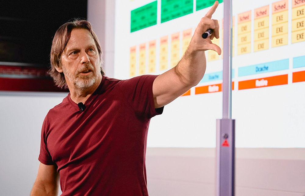
派对上最引人注目的人物在一群老朋友中显得悠然自得。他留着花白的胡子和冲浪手式的长发,身材很结实,看上去更像是一位已退役的橄榄球后卫或是职业冲浪手,而不像是设计了过去30年中最重要的芯片的设计师。他就是吉姆·凯勒,英特尔正在期待他能带领公司深陷困境的芯片设计业务重塑往日辉煌。
虽然凯勒在计算机行业之外鲜为人知,但在芯片制造领域,他绝对算得上是一位超级明星,地位堪比弗兰克·劳埃德·赖特在建筑领域的建树,或曾带领多支球队获取总冠军的篮球教练菲尔·杰克逊在NBA的影响力。凯勒的职业生涯开始于20世纪80年代,他最早在DEC公司就职,此后一步一步地取得了一系列令人瞩目的成就。他的设计帮助AMD公司从微芯片领域的失败者,发展成为令对手不可小觑的竞争者。而特斯拉全新的、能识别红绿灯和停车标志的芯片也是由凯勒设计的。苹果手机、谷歌云服务器和Xbox游戏机等产品的芯片,其核心技术都受到了凯勒的影响。在多年的工作历程中,凯勒也得以近距接触到史蒂夫·乔布斯、埃隆·马斯克,以及AMD公司创始人杰瑞·桑德斯等科技界传奇人物的管理风格。
AMD公司的前首席技术官弗雷德·韦伯说:“凯勒就像是科技行业的阿甘。他一直在做着最有趣的事情,一直在改变着世界。”2018年4月,这位“科技界阿甘”又踏上了新的旅程,离开特斯拉,加入了英特尔公司——而他此前的职业生涯中一直在同这家芯片行业巨头竞争。
凯勒是那场在哈德逊举办的派对上最重要的贵宾,连派对的举办地点都是他选的。他在派对上四处走动时,人们才惊讶地发现原来他很少谈论与芯片相关的话题。英特尔的服务器计算机架构师德布·伯恩斯坦很久以前也曾和凯勒一起在DEC公司共事。她回忆说,凯勒跟她讨论的是关于佛教和物理学的一些看法。(在与《财富》杂志的单独交流中,凯勒曾提到他从战斗机飞行员约翰·博伊德的传记以及精神教导书《不羁的灵魂》[The Untethered Soul]中学到的道理。)伯恩斯坦表示:“凯勒给人的感觉就像是他主动地通过不断学习,攻读了一个又一个的博士学位。”
在谈到自己的职业生涯时,凯勒本人也用教育做了一个类比。他把自己担任过的职位分成了两类:有的教会了他很多东西,有的则等着他去“执教”。他告诉《财富》杂志:“我在很多完全不同的企业工作过,我觉得自己在任职过每一家企业都学到了宝贵的经验教训。在加入苹果和特斯拉的时候,我没有想要去改变那里的任何事。我加入这样的企业是为了改变我自己。它们的工作方式跟世界上的很多其他企业都不一样。”
英特尔则属于凯勒提到的第二类企业——等着他去执教的企业。顶着技术、系统架构和客户部门高级副总裁的头衔,凯勒目前在英特尔的半导体工程部门管理着1万多名员工。英特尔的芯片研发此前遭遇了几次令人印象深刻的失败,企业的市场份额和利润也因此出现下滑趋势,而凯勒的工作则将决定英特尔能否重新成为下一代数据奇才和设备设计师眼中的霸主企业。
已在英特尔工作了近25年的公司平台研发事业部主管赛莱什·科塔帕利说:“我们正在经历着一次转型,而吉姆绝对是负责掌舵的最合适人选。我从未见过有着如此深厚技术背景的高管,他更有着技术方面的直觉。”
为了更深入地了解凯勒的直觉对他本人的影响,以及他的直觉可能将英特尔带向何方,《财富》杂志采访了30位凯勒的现任、前任同事以及竞争对手。(部分受访者由于未得到雇主许可而要求匿名接受我们的采访。)通过他们的描述,我们看到了一位极其天才的问题解决者的形象——他的职业生涯轨迹记录了过去30年内发生在计算机领域的若干重大变化。
从“内置英特尔”时代到深陷困境
微处理器设计领域十分重要,且一直在不断发展。1965年,英特尔的联合创始人戈登·摩尔首次提出了著名的摩尔定律,总结了制造领域技术进步的速度——在计算机芯片硅片尺寸不变的前提下,上面可以安装的晶体管数量却会越来越多。最新的苹果手机的A13仿生芯片在比一角硬币还要小的硅片上写入了85亿个晶体管。这使得芯片能够以越来越快的速度执行越来越多的功能,其应用领域也从计算机扩展到手机、汽车等产品,而现在甚至连灯柱和花园洒水器里都安装了芯片。
多亏了摩尔定律,现在芯片的设计和制造过程就好像是在一座已经建成的办公楼上添加新的楼层。仿佛突然之间,在价格不变的前提下,同一块地皮上就多出了不少大楼可供选择。但究竟该添加或改进些什么却不是一件显而易见的事。像凯勒这样的设计师必须紧跟任何可能提高处理器性能的硬件或软件趋势。他们还必须密切关注电脑用户究竟在做什么,从而预测他们的需求。更麻烦的是,有时候制造业的发展进步也会跟不上新芯片设计的需求。
过去十年里,这一复杂公式中的几个因素对英特尔产生了不利的影响。该公司一直在盈利——2019年,英特尔的营业收入达720亿美元,利润达210亿美元。但其增长有所放缓,市场份额也出现了下滑。英特尔的部分关键产品延迟上市,其重点关注的一些功能并不符合市场的需求,因此不得不放弃向昂贵的5G手机和平板电脑芯片领域进军。AMD和英伟达则在大型云数据中心芯片制造领域赶超了英特尔——该领域是增长最快、最有利可图的芯片市场之一。而对英特尔未来极为关键的一次收购——人工智能芯片初创公司Nervana,也未能取得预期的成功。(自去年12月以20亿美元的价格收购了Habana Labs之后,英特尔终止了Nervana处理器的开发工作,相当于承认收购失败,并决意重新开始。)
英特尔也在努力解决文化方面的问题。一些人认为,其巨大的规模和行业内的主导地位造就了一种官僚文化,导致企业运转缓慢、沟通不畅,还近乎病态地执迷于开发“万能型”产品,为每款新芯片添加过多的功能。这时的英特尔真正需要的,是一个新的关注点,以及更明智的领导层决策走向。而在芯片制造行业,没有人比吉姆·凯勒更擅长于专注和决策走向,更没有人比他更擅长于简化并解决问题。
________________________________________
芯片设计大神的书单
吉姆·凯勒的同事说他博览群书,能更好地从全新的角度来审视芯片设计。以下是凯勒最喜欢的一些读物以及他对于它们的评价。
《在数学中迷失》,作者:萨宾·霍森菲尔德
“很多我们以为是正确的事情其实是错误的,其中也包括不少物理学的内容,这一点非常出人意料。”
《不羁的灵魂》,作者:迈克尔·A·辛格
“这本书剖析了你内心的想法。当你把自己的想法拆解开来,认真去聆听的时候,是谁在聆听呢?接下来你又该怎么做?”
《博伊德:改变战争艺术的战斗机飞行员》,作者:罗伯特·科拉姆
美国空军飞行员约翰·博伊德“尽管面对着很多不同的问题,但每次都能想出新奇而有趣的解决方案。其中很多在技术和团队合作方面都很有用。”
________________________________________
数字教育
在这个现由斯坦福毕业生、麻省理工学院多学位毕业生以及少数哈佛肄业生主导的行业里,凯勒的教育背景显得很特别。凯勒在战后费城郊区的一片开发地区长大,由于患有阅读困难症,他到四年级时才开始识字。他很感激他的父母——他的父亲是通用电气航空航天公司的一名机械工程师,母亲是全职主妇。他们一直支持着他,鼓励他用好奇心探索世界,却不会给他过多的压力。
凯勒后来就读于宾夕法尼亚州立大学(他回忆说,麻省理工学院看起来好像“太难了”)。他知道自己想从事“科学相关,但又能赚到钱的事”。早些时候,他找到了一份大学各大专业平均起薪的清单。他最感兴趣的两个领域是生物学和物理学。但在清单里,这两个专业的起薪水平都在中间线之下,电气工程专业则名列前茅,因此他便选择了这个专业(他的第二专业是哲学)。幸运的是,凯勒的指导教师还负责运营学校的半导体实验室,所以凯勒很早就有机会接触到科技行业最重要的一个领域。
大学毕业后,凯勒迷茫了一小段时间,然后开始进入那个时代的科技巨头企业DEC工作。(《财富》杂志曾在1986年将DEC公司的创始人肯·奥尔森评为“本世纪最具影响力的企业家”,也许有点为时过早了。)20世纪80年代早期,凯勒刚刚开始工作的时候,DEC发展得非常快,吞噬着波士顿各处的办公空间;凯勒最早的办公室位于一家改建过的超市里。
与很多竞争对手不同,DEC公司选择自己制造芯片,而不是与外部供应商签约。这让凯勒很早就有机会接触到了计算机开发从设计到制造再到营销过程中的每一步。他了解了芯片如何布局,还参与构建了用来绘制芯片地图的CAD软件。这应该是他通过自学取得的第一个博士学位。他说:“那时候我有很多工具可以用。”
DEC公司最知名的产品之一,是一系列名为Alpha的处理器。Alpha处理器运行着所谓的工作站计算机,华尔街交易员、火箭科学家和气候模型专家都会使用这种强大的计算引擎,它们在计算机世界的食物链中处于个人电脑上游的位置。Alpha处理器则是工作站计算机中的速度型选手。《吉尼斯世界纪录》曾收到过DEC公司提交的几块Alpha处理器,并将它们评定为世界上最快的微处理器。凯勒本人参与设计了一款名为Alpha 21264的芯片,部分芯片的运行速度高达一千兆赫,这在当时是闻所未闻的。
尽管实力雄厚,到了20世纪90年代中期,DEC公司还是陷入了困境。该公司未能成功预见个人电脑和服务器会变得够快够强,足以令DEC的微型计算机过时。凯勒回忆说:“事实上,当时公司在制造着世界上最快的计算机,同时也在走向倒闭。”这段经历教会他一个难忘的教训:如果你制造的东西不是市场想要的,那么你造得再好也无关紧要。
最终,凯勒意识到,DEC的Alpha系列处理器面临着灭绝级别的挑战——对手正是英特尔。20世纪90年代中期,凯勒甚至拿到了英特尔当时全新的Pentium Pro(高能奔腾)处理器内部工作原理照片。就在哈德逊市,在英特尔为凯勒举办派对的那间房间里,当时的凯勒向同事们解释了英特尔划时代性的创造。英特尔长期采用的x86芯片设计此前运行的是来自软件程序的极其复杂的指令集:而在Pentium Pro中,英特尔找到了可以将程序指令快速转换成更简单的代码块的方法。英特尔的这项创造令Alpha处理器全部的优势不复存在,而这一天来得比所有人预期的都要快。
当时,英特尔在x86芯片制造领域的第二大竞争对手是AMD。凯勒在AMD也有熟人。他于1998年离开DEC并加入了AMD,此时他已经在DEC工作了14年。目前为止,DEC是他职业生涯中任职时间最久的一家公司。
在初创公司实现的突破
当时,美国AMD半导体公司的掌门人正是魅力十足的联合创始人兼首席执行官杰瑞·桑德斯。虽然桑德斯的销售技巧非常出色,但并不足以领导AMD在与英特尔的市场竞争中稳住阵脚。不过,吉姆·凯勒用一款名为K8的芯片,帮助AMD改变了这一状况。
随着芯片组的功能日渐强大,凯勒意识到,单独的芯片和电脑其它部分(如内存和存储)之间的运算出现了障碍。他还发现,随着各个部件都变得越来越小,可以将处理器与控制内存和数据传输的独立芯片集成在一起,从而简化芯片系统。他还有另一个简单化的设想:可以把两块处理器芯片放在一起,共享电脑主板上的一个插槽,从而加快与内存的交互速度。
在这样的创新之下,K8芯片不仅适用于普通个人电脑,也可以应用于服务器计算机这一新兴领域,在商业方面取得了相当的成绩;凯勒所做的集成还将极大地简化各个服务器的内部设置,为客户节省大量资金。
在那之前,桑德斯否决了为服务器开发芯片的提议,理由是AMD缺少开发服务器芯片所需的兼容性芯片组的支持生态系统。但凯勒对K8芯片的设计将主芯片上的芯片组功能整合在一起,巧妙地解决了这些问题。(凯勒在这个过程中一直很谨慎,他回忆说:“我记得,在告诉他这个项目对服务器也有好处之前,我们差不多已经完成了一半的工作。”)最后,同样重要的一点是,凯勒参与研发了一种超传输总线技术,让数据能在他的新K8芯片和其它服务器之间流动。
K8芯片助力推动了服务器行业的发展,注定会取得巨大的成功。经过多次更新之后,超传输标准仍然广泛地应用在服务器上,包括承载了亚马逊和谷歌云平台的芯片。
但凯勒没有在AMD待到能够庆祝胜利的时候。凯勒在DEC公司的一群前同事在Alpha处理器团队的工程师丹·多伯普尔的带领下,成立了一家名为SiByte的初创公司,当K8芯片还在研发的早期阶段时,凯勒收到了他们的邀请。所以,进入AMD仅一年之后,凯勒就跳了槽——这是他相对较短的一段工作时间,也成为了他职业生涯的一个特点。
对于设计者来说,在某一芯片的研发还处于这么早的阶段时就离开确实很不寻常,凯勒在AMD的部分团队成员对他的决定感到失望。几个月后,AMD的研发团队在一家高档法国小餐馆举办了一场鼓舞士气的宴会。宴会结束后,团队成员们当晚就回到了办公室,决定当场用大锤拆除一面将工程师和团队内其他成员隔开的墙。
当时担任AMD首席技术官的弗雷德·韦伯表示,那是一次团队建设活动,但也是对凯勒离职的失望之情的一种表达。韦伯在接受《财富》杂志采访时表示:“我绝不会说他没有做完什么事就走了——他肯定做了——但他早于大多数人离开了。他更像是一个提前结束项目的人。好消息是,他在前期做了很多事情,确定了一个很好的方向。”
凯勒在描述自己换工作的动机时则没那么委婉。“我是工程师的工程师。”他说。“工程师喜欢工作。我想把麻烦的问题解决掉,找一些明确的、有趣的问题来解决。”
K8芯片最终于2003年问世。芯片的官方名称为“皓龙”——但AMD公司还推出了一个名为“大锤”的版本。

陆地、海洋和天空
寻找需要解决的新问题也成为了凯勒闲暇时间的主要特征。在DEC时,随着资历和收入的增长,他开始购买一系列高性能轿跑车,并开着它们在路上高速行驶。他还迷上了风帆冲浪运动,经常和DEC公司的同事们踏上从波士顿到夏威夷的长途旅行,寻找最佳的冲浪场地。
某个周末,在DEC时曾在凯勒手下工作的丹·利勃霍兹来到他家,拜访自己的上司。在那之前,凯勒就已经教过他一些关于帆船的知识,但那天,他从车库里拿出了一套用于风帆冲浪的装备,将它交给了如今已成为亚德诺半导体技术公司(Analog Devices)首席技术官的利勃霍兹。“他想确定我真的会去做。”利勃霍兹回忆说。
凯勒在20世纪90年代末移居加州后,依然在追求海浪和高速公路的刺激。他的一些前同事回忆说,他经常在“自己定价”的旅游网站Priceline上竞拍去夏威夷的机票。以低价拍中之后,他就会去毛伊岛度过周末。凯勒在苹果公司工作了四年,公司鼓励员工在商务旅行时租用环保汽车,但凯勒却把这种租赁方式运用到了极限。有一次,他开着租来的混合动力车超速行驶,一位同事立即在凯勒办公室的门上正儿八经地贴了一张名牌,给他安了个“普锐斯赛车手”的头衔。
2010年代中期,凯勒又喜欢上了更具技术挑战性的风筝冲浪运动。他还学会了驾驶特技飞机。“我非常尊重他,但我不会和他一起跳进双座喷气式飞机。”约翰·伯恩回忆说。他曾是AMD负责市场和销售的高管,如今是戴尔公司北美地区的总负责人。而其他跟着上了飞机的人,则在凯勒带着他们在北加州的上空翻滚、垂直爬升时,努力克制着不要吐出来。
凯勒拒绝详细谈论对刺激运动的嗜好。但利勃霍兹认为风筝冲浪和凯勒在为芯片设计中棘手的问题寻找看似简单的解决方案的能力有些联系。风筝冲浪“是一项有趣的运动,同时也是一项技术含量极高、强度大、难度大的运动。”他说,“人在浪花上滑行,但在那表面之下,你所做的事情具有不可思议的深度和复杂性。”
在苹果吸取的经验
进入硅谷的选择使得凯勒一直处于芯片设计领域的中心。2000年11月,专注于研发网络处理器的SiByte被博通公司收购,凯勒得到了首席架构师的新职位。在这段时期,凯勒开创了所谓的双核设计,这象征着简化事业的又一次飞跃:本质上包含了同一块硅片上并排放置的两个计算芯片的核心,使得生成的芯片更快、更节能。博通公司将该芯片整合到路由器中,得以在全球范围内传输大量数据;到了2000年代后期,个人电脑也用上了双核芯片。
凯勒一直准备着迎接下一个有趣的问题。2004年,他加入了多伯普尔的另一家初创公司——P.A. Semi,这家公司专注于研发高端个人电脑和服务器的芯片。2008年,他跳槽到了苹果公司(就在苹果收购P.A. Semi之前)。对凯勒而言,“库比蒂诺之主”的吸引力有两点:一是能向世界上最顽强、最成功的首席执行官史蒂夫·乔布斯学习,二是能彻底投身于新兴的智能手机领域。
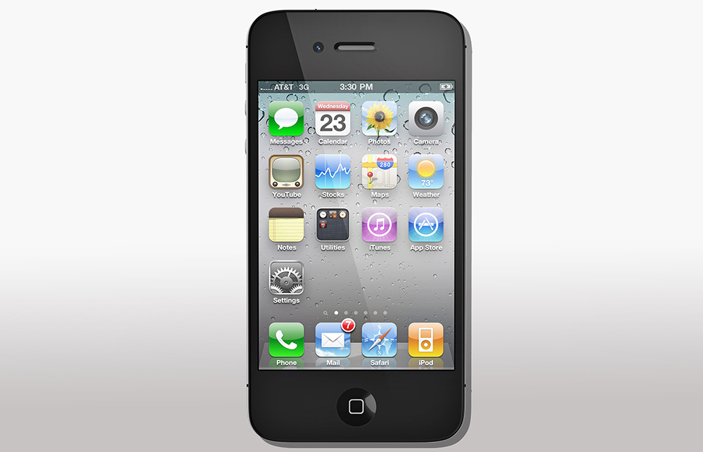
苹果公司的标志性产品iPhone的前三个版本使用的是三星的芯片:凯勒加入了一个负责设计苹果公司自己的芯片系列的团队。iPhone 4这款手机采用的就是凯勒参与研发的芯片。他对苹果A6和A7芯片的贡献最大,而这两款芯片为iPhone 5和5s提供了动力。这些芯片不只是比竞争对手的芯片更快:苹果还优化了显卡,使运行更加流畅。相比之下,iPhone的竞争对手就显得平平无奇了。这些芯片还加快了iPhone的语音处理速度——刚好为苹果公司新的数字助理Siri提供了动力。
凯勒并没有直接为乔布斯工作:他的上司鲍勃·曼斯菲尔德和迈克·卡尔伯特则能直接接触到那位要求严格、时而有些冲动的领导者。不过凯勒表示,他从乔布斯和曼斯菲尔德那里学到了很多关于“高强度工程”的知识。“他们的专注比我所见过的任何人都更精细。”凯勒回忆说。“就算是死也要达成计划目标。”凯勒还记住了乔布斯的一句格言,这句格言也呼应了凯勒许多成功的项目背后的原因:“一旦明白了什么事情应该做,就要一直做下去。”
到了2012年,凯勒已经准备好带着新见解回到自己的老东家AMD了。那时候,AMD已经失去了先前因为K8芯片而获得的技术领先地位,最先进的芯片也远远比不上英特尔最好的芯片。凯勒知道其中的缘故。他发现,AMD的芯片设计复杂,难以改进——他曾见过类似的情况,优秀的工程师可能会花过多时间忙于优化旧的芯片。
凯勒看到了重新开始的机会。芯片制造商的不断进步使得芯片的速度更快、功能更强,但也带来了新的问题:如今,最快的芯片往往非常容易过热,这将限制它们的运行速度。但凯勒发现了一种新的技术,可以帮助解决问题——使用“小芯片”。
从本质上说,小芯片就是芯片设计界的乐高积木:它们是体积更小、单独制造的硅块,可以合在一起组装成更大、更复杂的芯片。凯勒意识到他可以为计算密集型的活动——例如深度学习,或是图像丰富的视频游戏——制造新的芯片,而这只需要把几个芯片组装在一起。最终的成果比单个集成芯片更便宜,但功能依旧强大,且模块化的设置使得凯勒能够在不产生过多热量的情况下增强芯片的运算能力。随着云计算数据中心的需求与日俱增,这种芯片也适用于更宏大的配置。
要想将凯勒的想法变成现实,就意味着要从零开始,这引起了AMD公司内部的强烈反对。凯勒回忆说,人们当面告诉他,他会一败涂地;作为回应,他唤醒了了内心的那个史蒂夫·乔布斯。约翰·伯恩说,在一次市政厅会议上,凯勒变得非常激动,直接对人们的批评作出了回应。“他对他们说:‘这就是我们要做的事。我已经搭建好了架构。等着吧,你们会看到成果的。’”伯恩回忆说。“他有那种疯狂的专注。”
凯勒设计的第一组小芯片,也就是“锐龙”系列,直到2017年才上市。锐龙处理器的价格低于英特尔的芯片,并且从某种程度上来说,性能甚至还更好,因此一面世就立马引起了轰动。2019年时,第三代的锐龙芯片依然由凯勒设计,几乎在各个指标上都击败了竞争对手的芯片。顺理成章地,截至4月底,AMD的股价在五年内涨了2303%,投资回报率差不多是英特尔(上涨了78%)的30倍。
一如既往,当锐龙芯片真正上市的时候,凯勒早就离开AMD公司了。
四只轮子上的计算能力
这些年来,凯勒花了很多时间追求跑车的极限速度。但直到2015年,他听闻一些转投特斯拉的苹果前同事的提议,这才开始真正把汽车视为计算领域的挑战。特斯拉的创始人埃隆·马斯克想要打造自动驾驶汽车,而这个目标要求每辆车都具备强劲的计算性能。马斯克尝试过英特尔旗下Mobileye公司和英伟达的芯片,但两者都无法让他满意。
在一次相当于求职面试的会面中,凯勒说服了马斯克,称自己可以设计一款专利芯片,使它运行特斯拉自动驾驶软件的速度达到竞争对手的10倍。与此同时,马斯克也让凯勒相信,自己是那种可以帮助这位芯片设计师在他耀人的简历上再添一个“博士学位”的天才领袖。于是在2016年1月,凯勒正式履新。
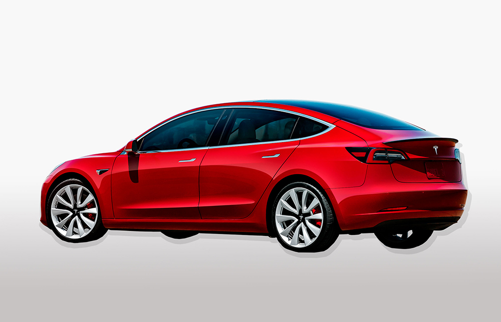
在特斯拉,凯勒成功的秘诀依旧是“化繁为简”。在掌握了特斯拉软件的运行机制后,他发现可以砍去或缩减英伟达芯片中与特斯拉软件无关的模块。2019年,凯勒设计的芯片开始被用于Model 3等车型。根据特斯拉的测算标准,新车性能是原来的20倍,也是凯勒之前许诺的两倍。尽管监管机构尚未放开对自动驾驶汽车的限制,但特斯拉的技术的确不同凡响:最近,特斯拉基于凯勒设计的芯片推出了一项新功能,Model 3只要识别到红灯和停车标志就可以自动停车。
凯勒还对特斯拉的生产线非常着迷。他喜欢在位于加州弗里蒙特的车间里闲逛,观看汽车的组装过程。这也让他有了一个发现:许多汽车零部件的寿命都能达到5或10年,但是为软件提供支持的电子芯片更换频率更高,可能每过两三年就得更新一次。于是,凯勒说服特斯拉重新设计了连接计算模块和其他部件的结构,让芯片板更加容易拆卸更新。有了新的结构,特斯拉如今才得以承诺凡是购买了自动驾驶功能的车辆,均可免费享受硬件升级服务。

最终加盟英特尔
到了2018年初,英特尔一再推迟新型芯片的量产时间,而且在平板电脑和5G领域举步维艰,因而越来越迫切地需要工程技术方面的帮助。正是这种艰难的处境吸引了凯勒。他离开特斯拉,并于2018年4月加入了恩怨数十载的“老冤家”英特尔麾下。
凯勒回忆说:“英特尔让我想起了DEC。它拥有卓越的技术和团队协作(文化),但有时候这种协作实在太离谱了。”他刚入职英特尔后参加了一场会议,会上有50个人就一个在他看来十分简单的问题展开了辩论。“如果这种事发生在特斯拉,埃隆会把所有人都杀了。”他说。通过他从马斯克和乔布斯那里得到的启示,凯勒一直在努力简化程序、精简团队规模、减少开会次数。他还换掉了自己所在部门所有负责管理工程师的非技术型经理。凯勒解释说:“要是把一个你遇到的问题告诉非技术型经理,那么(这个经理)只会又多了一个他解决不了的问题。”
参加工作近40年后,凯勒在英特尔不仅仅依靠他在数字设备公司认识的老同事。每加入一家公司,他都在不断拓展人脉。孙达丽·米特拉是芯片设计初创公司NetSpeed的联合创始人。她回忆了自己在2016年造访特斯拉,向凯勒展示本公司处理器设计方法时的情形。当团队开始演示第一张幻灯片时,凯勒就皱起了眉头。米特拉意识到,这是一位芯片领域的内行,他不需要、也不赞赏市场营销人员的那套鬼话。很快,两人就开始在白板上深入剖析方才的问题。米特拉回忆道:“吉姆并不关心层次有多高,他凭直觉就达到了那种高度。他想要的是第三层、第四层、第五层。”很快,凯勒就成了米特拉的导师。而在2018年9月,英特尔收购了NetSpeed公司,师徒俩也再度聚首。
对于他正在负责的重大芯片改造项目,凯勒并不愿详谈(芯片设计师一般都不愿介绍过多的细节),而英特尔的新芯片可能要等一至两年才能投入市场。尽管如此,英特尔公司和凯勒本人都透露了一些芯片结构方面的线索。新的芯片将清晰划分几个主要功能,便于公司一次改进一个部分——这种方法也让人联想到凯勒在AMD使用的“小芯片”模型。凯勒还暗示说,在他的个人电脑和服务器芯片设计中,英特尔的低功耗Atom芯片系列可能会占据更重要的位置。人工智能芯片的性能显然也被提上了议程:凯勒经常会参加人工智能方面的研讨会,他阅读了大量资料,尽可能地了解未来5年或10年内人工智能应用领域的发展方向。
英特尔也有可能会使用外部厂商的技术来实现部分功能,而不是像过去那样全程自主研发。凯勒所在工程部门的一名副总裁博伊德·菲尔普斯表示:“在凯勒加盟以前,可能我们都不会做出这样的改变。”
至于凯勒能否像他在那么多老东家那儿一样,也在英特尔取得成功,分析人士的意见并不一致。伯恩斯坦研究公司的分析师斯泰西·拉斯根说:“他们需要一些重磅产品,这是肯定的,而(凯勒)就是个重磅人物。不知道他会怎么处理那么多历史遗留问题,过几年再看看吧。”
当然了,凯勒向来擅长把历史遗留问题变得更轻盈、更简单、更流畅。当美国大部分地区实行了封锁措施后,凯勒在他位于硅谷的家中接受了《财富》杂志的电话采访。他的两个十几岁的女儿正忙着应付在线课程,但凯勒并不担心。他说:“很快就会恢复正常的,人类会解决所有的问题。”而有些人解决问题的速度比别人快得多。
全明星芯片阵容
在近40年的职业生涯里,吉姆·凯勒设计了不少科技行业最出色、最富有开拓性的微芯片。以下是他的几款主要作品及其上市年份。
Digital Alpha 21264处理器(1996年)
这是第一款主频达到500兆赫的芯片,其中,内存缓存达到了史无前例的1千兆赫。为了提高性能,Alpha处理器还开创了乱序执行软件指令的先河。

AMD皓龙处理器(2003年)
AMD皓龙是第一批64位处理器。它主要用于服务器,并开创了一种名为HyperTransport的数据传输标准。这种标准至今仍在云计算领域得到广泛应用。
苹果A4处理器(2010年)
凯勒当时专注于提高图形处理能力。这枚用于初代iPad和iPhone 4的芯片让苹果公司的第一款高分辨率“retina”显示屏成为可能。
特斯拉Autopilot(2019年)
特斯拉表示,公司首款用于自动驾驶的内部人工智能芯片,其运行速度是原有英伟达芯片的20倍。
英特尔Tremont(2020年)
Tremont是第一批受到凯勒影响的英特尔处理器。这种低功耗芯片适用于小型便携式设备,但也可以扩展到个人电脑。(财富中文网)
译者:Shog
去年初春的一天,在位于波士顿以西约50公里、马萨诸塞州哈德逊市的一片田园风光山坡上,半导体巨头企业英特尔为公司的30多名设计师、工程师和其他员工举办了一场派对。
依照科技行业的标准,派对上的这群人显得比较成熟——大部分人都穿着马球衫、开襟针织衫或衬衣,很少有人穿连帽衫。事实上,他们中的大多数人在20世纪90年代中期或者更早的时候就进入科技行业工作了。加入英特尔之前,他们还曾在数字设备公司(DEC)工作过——现已不复存在的DEC曾是一家开创性的科技巨头企业,举办这场派对的地方以前曾为DEC所有。
派对上最引人注目的人物在一群老朋友中显得悠然自得。他留着花白的胡子和冲浪手式的长发,身材很结实,看上去更像是一位已退役的橄榄球后卫或是职业冲浪手,而不像是设计了过去30年中最重要的芯片的设计师。他就是吉姆·凯勒,英特尔正在期待他能带领公司深陷困境的芯片设计业务重塑往日辉煌。
虽然凯勒在计算机行业之外鲜为人知,但在芯片制造领域,他绝对算得上是一位超级明星,地位堪比弗兰克·劳埃德·赖特在建筑领域的建树,或曾带领多支球队获取总冠军的篮球教练菲尔·杰克逊在NBA的影响力。凯勒的职业生涯开始于20世纪80年代,他最早在DEC公司就职,此后一步一步地取得了一系列令人瞩目的成就。他的设计帮助AMD公司从微芯片领域的失败者,发展成为令对手不可小觑的竞争者。而特斯拉全新的、能识别红绿灯和停车标志的芯片也是由凯勒设计的。苹果手机、谷歌云服务器和Xbox游戏机等产品的芯片,其核心技术都受到了凯勒的影响。在多年的工作历程中,凯勒也得以近距接触到史蒂夫·乔布斯、埃隆·马斯克,以及AMD公司创始人杰瑞·桑德斯等科技界传奇人物的管理风格。
AMD公司的前首席技术官弗雷德·韦伯说:“凯勒就像是科技行业的阿甘。他一直在做着最有趣的事情,一直在改变着世界。”2018年4月,这位“科技界阿甘”又踏上了新的旅程,离开特斯拉,加入了英特尔公司——而他此前的职业生涯中一直在同这家芯片行业巨头竞争。
凯勒是那场在哈德逊举办的派对上最重要的贵宾,连派对的举办地点都是他选的。他在派对上四处走动时,人们才惊讶地发现原来他很少谈论与芯片相关的话题。英特尔的服务器计算机架构师德布·伯恩斯坦很久以前也曾和凯勒一起在DEC公司共事。她回忆说,凯勒跟她讨论的是关于佛教和物理学的一些看法。(在与《财富》杂志的单独交流中,凯勒曾提到他从战斗机飞行员约翰·博伊德的传记以及精神教导书《不羁的灵魂》[The Untethered Soul]中学到的道理。)伯恩斯坦表示:“凯勒给人的感觉就像是他主动地通过不断学习,攻读了一个又一个的博士学位。”
在谈到自己的职业生涯时,凯勒本人也用教育做了一个类比。他把自己担任过的职位分成了两类:有的教会了他很多东西,有的则等着他去“执教”。他告诉《财富》杂志:“我在很多完全不同的企业工作过,我觉得自己在任职过每一家企业都学到了宝贵的经验教训。在加入苹果和特斯拉的时候,我没有想要去改变那里的任何事。我加入这样的企业是为了改变我自己。它们的工作方式跟世界上的很多其他企业都不一样。”
英特尔则属于凯勒提到的第二类企业——等着他去执教的企业。顶着技术、系统架构和客户部门高级副总裁的头衔,凯勒目前在英特尔的半导体工程部门管理着1万多名员工。英特尔的芯片研发此前遭遇了几次令人印象深刻的失败,企业的市场份额和利润也因此出现下滑趋势,而凯勒的工作则将决定英特尔能否重新成为下一代数据奇才和设备设计师眼中的霸主企业。
已在英特尔工作了近25年的公司平台研发事业部主管赛莱什·科塔帕利说:“我们正在经历着一次转型,而吉姆绝对是负责掌舵的最合适人选。我从未见过有着如此深厚技术背景的高管,他更有着技术方面的直觉。”
为了更深入地了解凯勒的直觉对他本人的影响,以及他的直觉可能将英特尔带向何方,《财富》杂志采访了30位凯勒的现任、前任同事以及竞争对手。(部分受访者由于未得到雇主许可而要求匿名接受我们的采访。)通过他们的描述,我们看到了一位极其天才的问题解决者的形象——他的职业生涯轨迹记录了过去30年内发生在计算机领域的若干重大变化。
从“内置英特尔”时代到深陷困境
微处理器设计领域十分重要,且一直在不断发展。1965年,英特尔的联合创始人戈登·摩尔首次提出了著名的摩尔定律,总结了制造领域技术进步的速度——在计算机芯片硅片尺寸不变的前提下,上面可以安装的晶体管数量却会越来越多。最新的苹果手机的A13仿生芯片在比一角硬币还要小的硅片上写入了85亿个晶体管。这使得芯片能够以越来越快的速度执行越来越多的功能,其应用领域也从计算机扩展到手机、汽车等产品,而现在甚至连灯柱和花园洒水器里都安装了芯片。
多亏了摩尔定律,现在芯片的设计和制造过程就好像是在一座已经建成的办公楼上添加新的楼层。仿佛突然之间,在价格不变的前提下,同一块地皮上就多出了不少大楼可供选择。但究竟该添加或改进些什么却不是一件显而易见的事。像凯勒这样的设计师必须紧跟任何可能提高处理器性能的硬件或软件趋势。他们还必须密切关注电脑用户究竟在做什么,从而预测他们的需求。更麻烦的是,有时候制造业的发展进步也会跟不上新芯片设计的需求。
过去十年里,这一复杂公式中的几个因素对英特尔产生了不利的影响。该公司一直在盈利——2019年,英特尔的营业收入达720亿美元,利润达210亿美元。但其增长有所放缓,市场份额也出现了下滑。英特尔的部分关键产品延迟上市,其重点关注的一些功能并不符合市场的需求,因此不得不放弃向昂贵的5G手机和平板电脑芯片领域进军。AMD和英伟达则在大型云数据中心芯片制造领域赶超了英特尔——该领域是增长最快、最有利可图的芯片市场之一。而对英特尔未来极为关键的一次收购——人工智能芯片初创公司Nervana,也未能取得预期的成功。(自去年12月以20亿美元的价格收购了Habana Labs之后,英特尔终止了Nervana处理器的开发工作,相当于承认收购失败,并决意重新开始。)
英特尔也在努力解决文化方面的问题。一些人认为,其巨大的规模和行业内的主导地位造就了一种官僚文化,导致企业运转缓慢、沟通不畅,还近乎病态地执迷于开发“万能型”产品,为每款新芯片添加过多的功能。这时的英特尔真正需要的,是一个新的关注点,以及更明智的领导层决策走向。而在芯片制造行业,没有人比吉姆·凯勒更擅长于专注和决策走向,更没有人比他更擅长于简化并解决问题。
芯片设计大神的书单
吉姆·凯勒的同事说他博览群书,能更好地从全新的角度来审视芯片设计。以下是凯勒最喜欢的一些读物以及他对于它们的评价。
《在数学中迷失》,作者:萨宾·霍森菲尔德
“很多我们以为是正确的事情其实是错误的,其中也包括不少物理学的内容,这一点非常出人意料。”
《不羁的灵魂》,作者:迈克尔·A·辛格
“这本书剖析了你内心的想法。当你把自己的想法拆解开来,认真去聆听的时候,是谁在聆听呢?接下来你又该怎么做?”
《博伊德:改变战争艺术的战斗机飞行员》,作者:罗伯特·科拉姆
美国空军飞行员约翰·博伊德“尽管面对着很多不同的问题,但每次都能想出新奇而有趣的解决方案。其中很多在技术和团队合作方面都很有用。”
数字教育
在这个现由斯坦福毕业生、麻省理工学院多学位毕业生以及少数哈佛肄业生主导的行业里,凯勒的教育背景显得很特别。凯勒在战后费城郊区的一片开发地区长大,由于患有阅读困难症,他到四年级时才开始识字。他很感激他的父母——他的父亲是通用电气航空航天公司的一名机械工程师,母亲是全职主妇。他们一直支持着他,鼓励他用好奇心探索世界,却不会给他过多的压力。
凯勒后来就读于宾夕法尼亚州立大学(他回忆说,麻省理工学院看起来好像“太难了”)。他知道自己想从事“科学相关,但又能赚到钱的事”。早些时候,他找到了一份大学各大专业平均起薪的清单。他最感兴趣的两个领域是生物学和物理学。但在清单里,这两个专业的起薪水平都在中间线之下,电气工程专业则名列前茅,因此他便选择了这个专业(他的第二专业是哲学)。幸运的是,凯勒的指导教师还负责运营学校的半导体实验室,所以凯勒很早就有机会接触到科技行业最重要的一个领域。
大学毕业后,凯勒迷茫了一小段时间,然后开始进入那个时代的科技巨头企业DEC工作。(《财富》杂志曾在1986年将DEC公司的创始人肯·奥尔森评为“本世纪最具影响力的企业家”,也许有点为时过早了。)20世纪80年代早期,凯勒刚刚开始工作的时候,DEC发展得非常快,吞噬着波士顿各处的办公空间;凯勒最早的办公室位于一家改建过的超市里。
与很多竞争对手不同,DEC公司选择自己制造芯片,而不是与外部供应商签约。这让凯勒很早就有机会接触到了计算机开发从设计到制造再到营销过程中的每一步。他了解了芯片如何布局,还参与构建了用来绘制芯片地图的CAD软件。这应该是他通过自学取得的第一个博士学位。他说:“那时候我有很多工具可以用。”
DEC公司最知名的产品之一,是一系列名为Alpha的处理器。Alpha处理器运行着所谓的工作站计算机,华尔街交易员、火箭科学家和气候模型专家都会使用这种强大的计算引擎,它们在计算机世界的食物链中处于个人电脑上游的位置。Alpha处理器则是工作站计算机中的速度型选手。《吉尼斯世界纪录》曾收到过DEC公司提交的几块Alpha处理器,并将它们评定为世界上最快的微处理器。凯勒本人参与设计了一款名为Alpha 21264的芯片,部分芯片的运行速度高达一千兆赫,这在当时是闻所未闻的。
尽管实力雄厚,到了20世纪90年代中期,DEC公司还是陷入了困境。该公司未能成功预见个人电脑和服务器会变得够快够强,足以令DEC的微型计算机过时。凯勒回忆说:“事实上,当时公司在制造着世界上最快的计算机,同时也在走向倒闭。”这段经历教会他一个难忘的教训:如果你制造的东西不是市场想要的,那么你造得再好也无关紧要。
最终,凯勒意识到,DEC的Alpha系列处理器面临着灭绝级别的挑战——对手正是英特尔。20世纪90年代中期,凯勒甚至拿到了英特尔当时全新的Pentium Pro(高能奔腾)处理器内部工作原理照片。就在哈德逊市,在英特尔为凯勒举办派对的那间房间里,当时的凯勒向同事们解释了英特尔划时代性的创造。英特尔长期采用的x86芯片设计此前运行的是来自软件程序的极其复杂的指令集:而在Pentium Pro中,英特尔找到了可以将程序指令快速转换成更简单的代码块的方法。英特尔的这项创造令Alpha处理器全部的优势不复存在,而这一天来得比所有人预期的都要快。
当时,英特尔在x86芯片制造领域的第二大竞争对手是AMD。凯勒在AMD也有熟人。他于1998年离开DEC并加入了AMD,此时他已经在DEC工作了14年。目前为止,DEC是他职业生涯中任职时间最久的一家公司。
在初创公司实现的突破
当时,美国AMD半导体公司的掌门人正是魅力十足的联合创始人兼首席执行官杰瑞·桑德斯。虽然桑德斯的销售技巧非常出色,但并不足以领导AMD在与英特尔的市场竞争中稳住阵脚。不过,吉姆·凯勒用一款名为K8的芯片,帮助AMD改变了这一状况。
随着芯片组的功能日渐强大,凯勒意识到,单独的芯片和电脑其它部分(如内存和存储)之间的运算出现了障碍。他还发现,随着各个部件都变得越来越小,可以将处理器与控制内存和数据传输的独立芯片集成在一起,从而简化芯片系统。他还有另一个简单化的设想:可以把两块处理器芯片放在一起,共享电脑主板上的一个插槽,从而加快与内存的交互速度。
在这样的创新之下,K8芯片不仅适用于普通个人电脑,也可以应用于服务器计算机这一新兴领域,在商业方面取得了相当的成绩;凯勒所做的集成还将极大地简化各个服务器的内部设置,为客户节省大量资金。
在那之前,桑德斯否决了为服务器开发芯片的提议,理由是AMD缺少开发服务器芯片所需的兼容性芯片组的支持生态系统。但凯勒对K8芯片的设计将主芯片上的芯片组功能整合在一起,巧妙地解决了这些问题。(凯勒在这个过程中一直很谨慎,他回忆说:“我记得,在告诉他这个项目对服务器也有好处之前,我们差不多已经完成了一半的工作。”)最后,同样重要的一点是,凯勒参与研发了一种超传输总线技术,让数据能在他的新K8芯片和其它服务器之间流动。
K8芯片助力推动了服务器行业的发展,注定会取得巨大的成功。经过多次更新之后,超传输标准仍然广泛地应用在服务器上,包括承载了亚马逊和谷歌云平台的芯片。
但凯勒没有在AMD待到能够庆祝胜利的时候。凯勒在DEC公司的一群前同事在Alpha处理器团队的工程师丹·多伯普尔的带领下,成立了一家名为SiByte的初创公司,当K8芯片还在研发的早期阶段时,凯勒收到了他们的邀请。所以,进入AMD仅一年之后,凯勒就跳了槽——这是他相对较短的一段工作时间,也成为了他职业生涯的一个特点。
对于设计者来说,在某一芯片的研发还处于这么早的阶段时就离开确实很不寻常,凯勒在AMD的部分团队成员对他的决定感到失望。几个月后,AMD的研发团队在一家高档法国小餐馆举办了一场鼓舞士气的宴会。宴会结束后,团队成员们当晚就回到了办公室,决定当场用大锤拆除一面将工程师和团队内其他成员隔开的墙。
当时担任AMD首席技术官的弗雷德·韦伯表示,那是一次团队建设活动,但也是对凯勒离职的失望之情的一种表达。韦伯在接受《财富》杂志采访时表示:“我绝不会说他没有做完什么事就走了——他肯定做了——但他早于大多数人离开了。他更像是一个提前结束项目的人。好消息是,他在前期做了很多事情,确定了一个很好的方向。”
凯勒在描述自己换工作的动机时则没那么委婉。“我是工程师的工程师。”他说。“工程师喜欢工作。我想把麻烦的问题解决掉,找一些明确的、有趣的问题来解决。”
K8芯片最终于2003年问世。芯片的官方名称为“皓龙”——但AMD公司还推出了一个名为“大锤”的版本。
陆地、海洋和天空
寻找需要解决的新问题也成为了凯勒闲暇时间的主要特征。在DEC时,随着资历和收入的增长,他开始购买一系列高性能轿跑车,并开着它们在路上高速行驶。他还迷上了风帆冲浪运动,经常和DEC公司的同事们踏上从波士顿到夏威夷的长途旅行,寻找最佳的冲浪场地。
某个周末,在DEC时曾在凯勒手下工作的丹·利勃霍兹来到他家,拜访自己的上司。在那之前,凯勒就已经教过他一些关于帆船的知识,但那天,他从车库里拿出了一套用于风帆冲浪的装备,将它交给了如今已成为亚德诺半导体技术公司(Analog Devices)首席技术官的利勃霍兹。“他想确定我真的会去做。”利勃霍兹回忆说。
凯勒在20世纪90年代末移居加州后,依然在追求海浪和高速公路的刺激。他的一些前同事回忆说,他经常在“自己定价”的旅游网站Priceline上竞拍去夏威夷的机票。以低价拍中之后,他就会去毛伊岛度过周末。凯勒在苹果公司工作了四年,公司鼓励员工在商务旅行时租用环保汽车,但凯勒却把这种租赁方式运用到了极限。有一次,他开着租来的混合动力车超速行驶,一位同事立即在凯勒办公室的门上正儿八经地贴了一张名牌,给他安了个“普锐斯赛车手”的头衔。
2010年代中期,凯勒又喜欢上了更具技术挑战性的风筝冲浪运动。他还学会了驾驶特技飞机。“我非常尊重他,但我不会和他一起跳进双座喷气式飞机。”约翰·伯恩回忆说。他曾是AMD负责市场和销售的高管,如今是戴尔公司北美地区的总负责人。而其他跟着上了飞机的人,则在凯勒带着他们在北加州的上空翻滚、垂直爬升时,努力克制着不要吐出来。
凯勒拒绝详细谈论对刺激运动的嗜好。但利勃霍兹认为风筝冲浪和凯勒在为芯片设计中棘手的问题寻找看似简单的解决方案的能力有些联系。风筝冲浪“是一项有趣的运动,同时也是一项技术含量极高、强度大、难度大的运动。”他说,“人在浪花上滑行,但在那表面之下,你所做的事情具有不可思议的深度和复杂性。”
在苹果吸取的经验
进入硅谷的选择使得凯勒一直处于芯片设计领域的中心。2000年11月,专注于研发网络处理器的SiByte被博通公司收购,凯勒得到了首席架构师的新职位。在这段时期,凯勒开创了所谓的双核设计,这象征着简化事业的又一次飞跃:本质上包含了同一块硅片上并排放置的两个计算芯片的核心,使得生成的芯片更快、更节能。博通公司将该芯片整合到路由器中,得以在全球范围内传输大量数据;到了2000年代后期,个人电脑也用上了双核芯片。
凯勒一直准备着迎接下一个有趣的问题。2004年,他加入了多伯普尔的另一家初创公司——P.A. Semi,这家公司专注于研发高端个人电脑和服务器的芯片。2008年,他跳槽到了苹果公司(就在苹果收购P.A. Semi之前)。对凯勒而言,“库比蒂诺之主”的吸引力有两点:一是能向世界上最顽强、最成功的首席执行官史蒂夫·乔布斯学习,二是能彻底投身于新兴的智能手机领域。
苹果公司的标志性产品iPhone的前三个版本使用的是三星的芯片:凯勒加入了一个负责设计苹果公司自己的芯片系列的团队。iPhone 4这款手机采用的就是凯勒参与研发的芯片。他对苹果A6和A7芯片的贡献最大,而这两款芯片为iPhone 5和5s提供了动力。这些芯片不只是比竞争对手的芯片更快:苹果还优化了显卡,使运行更加流畅。相比之下,iPhone的竞争对手就显得平平无奇了。这些芯片还加快了iPhone的语音处理速度——刚好为苹果公司新的数字助理Siri提供了动力。
凯勒并没有直接为乔布斯工作:他的上司鲍勃·曼斯菲尔德和迈克·卡尔伯特则能直接接触到那位要求严格、时而有些冲动的领导者。不过凯勒表示,他从乔布斯和曼斯菲尔德那里学到了很多关于“高强度工程”的知识。“他们的专注比我所见过的任何人都更精细。”凯勒回忆说。“就算是死也要达成计划目标。”凯勒还记住了乔布斯的一句格言,这句格言也呼应了凯勒许多成功的项目背后的原因:“一旦明白了什么事情应该做,就要一直做下去。”
到了2012年,凯勒已经准备好带着新见解回到自己的老东家AMD了。那时候,AMD已经失去了先前因为K8芯片而获得的技术领先地位,最先进的芯片也远远比不上英特尔最好的芯片。凯勒知道其中的缘故。他发现,AMD的芯片设计复杂,难以改进——他曾见过类似的情况,优秀的工程师可能会花过多时间忙于优化旧的芯片。
凯勒看到了重新开始的机会。芯片制造商的不断进步使得芯片的速度更快、功能更强,但也带来了新的问题:如今,最快的芯片往往非常容易过热,这将限制它们的运行速度。但凯勒发现了一种新的技术,可以帮助解决问题——使用“小芯片”。
从本质上说,小芯片就是芯片设计界的乐高积木:它们是体积更小、单独制造的硅块,可以合在一起组装成更大、更复杂的芯片。凯勒意识到他可以为计算密集型的活动——例如深度学习,或是图像丰富的视频游戏——制造新的芯片,而这只需要把几个芯片组装在一起。最终的成果比单个集成芯片更便宜,但功能依旧强大,且模块化的设置使得凯勒能够在不产生过多热量的情况下增强芯片的运算能力。随着云计算数据中心的需求与日俱增,这种芯片也适用于更宏大的配置。
要想将凯勒的想法变成现实,就意味着要从零开始,这引起了AMD公司内部的强烈反对。凯勒回忆说,人们当面告诉他,他会一败涂地;作为回应,他唤醒了了内心的那个史蒂夫·乔布斯。约翰·伯恩说,在一次市政厅会议上,凯勒变得非常激动,直接对人们的批评作出了回应。“他对他们说:‘这就是我们要做的事。我已经搭建好了架构。等着吧,你们会看到成果的。’”伯恩回忆说。“他有那种疯狂的专注。”
凯勒设计的第一组小芯片,也就是“锐龙”系列,直到2017年才上市。锐龙处理器的价格低于英特尔的芯片,并且从某种程度上来说,性能甚至还更好,因此一面世就立马引起了轰动。2019年时,第三代的锐龙芯片依然由凯勒设计,几乎在各个指标上都击败了竞争对手的芯片。顺理成章地,截至4月底,AMD的股价在五年内涨了2303%,投资回报率差不多是英特尔(上涨了78%)的30倍。
一如既往,当锐龙芯片真正上市的时候,凯勒早就离开AMD公司了。
四只轮子上的计算能力
这些年来,凯勒花了很多时间追求跑车的极限速度。但直到2015年,他听闻一些转投特斯拉的苹果前同事的提议,这才开始真正把汽车视为计算领域的挑战。特斯拉的创始人埃隆·马斯克想要打造自动驾驶汽车,而这个目标要求每辆车都具备强劲的计算性能。马斯克尝试过英特尔旗下Mobileye公司和英伟达的芯片,但两者都无法让他满意。
在一次相当于求职面试的会面中,凯勒说服了马斯克,称自己可以设计一款专利芯片,使它运行特斯拉自动驾驶软件的速度达到竞争对手的10倍。与此同时,马斯克也让凯勒相信,自己是那种可以帮助这位芯片设计师在他耀人的简历上再添一个“博士学位”的天才领袖。于是在2016年1月,凯勒正式履新。
在特斯拉,凯勒成功的秘诀依旧是“化繁为简”。在掌握了特斯拉软件的运行机制后,他发现可以砍去或缩减英伟达芯片中与特斯拉软件无关的模块。2019年,凯勒设计的芯片开始被用于Model 3等车型。根据特斯拉的测算标准,新车性能是原来的20倍,也是凯勒之前许诺的两倍。尽管监管机构尚未放开对自动驾驶汽车的限制,但特斯拉的技术的确不同凡响:最近,特斯拉基于凯勒设计的芯片推出了一项新功能,Model 3只要识别到红灯和停车标志就可以自动停车。
凯勒还对特斯拉的生产线非常着迷。他喜欢在位于加州弗里蒙特的车间里闲逛,观看汽车的组装过程。这也让他有了一个发现:许多汽车零部件的寿命都能达到5或10年,但是为软件提供支持的电子芯片更换频率更高,可能每过两三年就得更新一次。于是,凯勒说服特斯拉重新设计了连接计算模块和其他部件的结构,让芯片板更加容易拆卸更新。有了新的结构,特斯拉如今才得以承诺凡是购买了自动驾驶功能的车辆,均可免费享受硬件升级服务。
最终加盟英特尔
到了2018年初,英特尔一再推迟新型芯片的量产时间,而且在平板电脑和5G领域举步维艰,因而越来越迫切地需要工程技术方面的帮助。正是这种艰难的处境吸引了凯勒。他离开特斯拉,并于2018年4月加入了恩怨数十载的“老冤家”英特尔麾下。
凯勒回忆说:“英特尔让我想起了DEC。它拥有卓越的技术和团队协作(文化),但有时候这种协作实在太离谱了。”他刚入职英特尔后参加了一场会议,会上有50个人就一个在他看来十分简单的问题展开了辩论。“如果这种事发生在特斯拉,埃隆会把所有人都杀了。”他说。通过他从马斯克和乔布斯那里得到的启示,凯勒一直在努力简化程序、精简团队规模、减少开会次数。他还换掉了自己所在部门所有负责管理工程师的非技术型经理。凯勒解释说:“要是把一个你遇到的问题告诉非技术型经理,那么(这个经理)只会又多了一个他解决不了的问题。”
参加工作近40年后,凯勒在英特尔不仅仅依靠他在数字设备公司认识的老同事。每加入一家公司,他都在不断拓展人脉。孙达丽·米特拉是芯片设计初创公司NetSpeed的联合创始人。她回忆了自己在2016年造访特斯拉,向凯勒展示本公司处理器设计方法时的情形。当团队开始演示第一张幻灯片时,凯勒就皱起了眉头。米特拉意识到,这是一位芯片领域的内行,他不需要、也不赞赏市场营销人员的那套鬼话。很快,两人就开始在白板上深入剖析方才的问题。米特拉回忆道:“吉姆并不关心层次有多高,他凭直觉就达到了那种高度。他想要的是第三层、第四层、第五层。”很快,凯勒就成了米特拉的导师。而在2018年9月,英特尔收购了NetSpeed公司,师徒俩也再度聚首。
对于他正在负责的重大芯片改造项目,凯勒并不愿详谈(芯片设计师一般都不愿介绍过多的细节),而英特尔的新芯片可能要等一至两年才能投入市场。尽管如此,英特尔公司和凯勒本人都透露了一些芯片结构方面的线索。新的芯片将清晰划分几个主要功能,便于公司一次改进一个部分——这种方法也让人联想到凯勒在AMD使用的“小芯片”模型。凯勒还暗示说,在他的个人电脑和服务器芯片设计中,英特尔的低功耗Atom芯片系列可能会占据更重要的位置。人工智能芯片的性能显然也被提上了议程:凯勒经常会参加人工智能方面的研讨会,他阅读了大量资料,尽可能地了解未来5年或10年内人工智能应用领域的发展方向。
英特尔也有可能会使用外部厂商的技术来实现部分功能,而不是像过去那样全程自主研发。凯勒所在工程部门的一名副总裁博伊德·菲尔普斯表示:“在凯勒加盟以前,可能我们都不会做出这样的改变。”
至于凯勒能否像他在那么多老东家那儿一样,也在英特尔取得成功,分析人士的意见并不一致。伯恩斯坦研究公司的分析师斯泰西·拉斯根说:“他们需要一些重磅产品,这是肯定的,而(凯勒)就是个重磅人物。不知道他会怎么处理那么多历史遗留问题,过几年再看看吧。”
当然了,凯勒向来擅长把历史遗留问题变得更轻盈、更简单、更流畅。当美国大部分地区实行了封锁措施后,凯勒在他位于硅谷的家中接受了《财富》杂志的电话采访。他的两个十几岁的女儿正忙着应付在线课程,但凯勒并不担心。他说:“很快就会恢复正常的,人类会解决所有的问题。”而有些人解决问题的速度比别人快得多。
全明星芯片阵容
在近40年的职业生涯里,吉姆·凯勒设计了不少科技行业最出色、最富有开拓性的微芯片。以下是他的几款主要作品及其上市年份。
Digital Alpha 21264处理器(1996年)
这是第一款主频达到500兆赫的芯片,其中,内存缓存达到了史无前例的1千兆赫。为了提高性能,Alpha处理器还开创了乱序执行软件指令的先河。
AMD皓龙处理器(2003年)
AMD皓龙是第一批64位处理器。它主要用于服务器,并开创了一种名为HyperTransport的数据传输标准。这种标准至今仍在云计算领域得到广泛应用。
苹果A4处理器(2010年)
凯勒当时专注于提高图形处理能力。这枚用于初代iPad和iPhone 4的芯片让苹果公司的第一款高分辨率“retina”显示屏成为可能。
特斯拉Autopilot(2019年)
特斯拉表示,公司首款用于自动驾驶的内部人工智能芯片,其运行速度是原有英伟达芯片的20倍。
英特尔Tremont(2020年)
Tremont是第一批受到凯勒影响的英特尔处理器。这种低功耗芯片适用于小型便携式设备,但也可以扩展到个人电脑。(财富中文网)
译者:Shog
On a bucolic hillside in Hudson, Mass., about 30 miles west of Boston, on an early spring day last year, the semiconductor giant Intel threw a party for more than 30 of its designers, engineers, and other employees.
It was a pretty mature group, by tech industry standards—lots of polo shirts, cardigans and button-downs, very few hoodies. Indeed, virtually everyone in the crowd had been in tech since the mid-1990s or earlier. Before their Intel days, the partygoers had worked for Digital Equipment Corp., or DEC—a pioneering but long-gone tech giant that had once owned the very building that was hosting the party.
At the center of attention, mingling easily with old friends, was a man with a graying beard, beach-appropriate longish hair, and a muscular build—someone who looked more like a retired linebacker or professional surfer than the architect of some of the most important microchip designs of the past 30 years. The man was Jim Keller, the person Intel is counting on to revitalize its own struggling chip-design enterprise.
Though he is little known outside the computer industry, Keller is a chipmaking superstar, on the level of Frank Lloyd Wright in building architecture—or comparable to NBA coach Phil Jackson for the teams he has led to success. In a career that began at DEC in the 1980s, Keller has racked up remarkable achievements at stop after stop. His designs helped turn Advanced Micro Devices from a microchip also-ran into a respected contender. The autopilot chip in new Teslas that can recognize red lights and stop signs? That’s a Keller design. And the chips in everything from iPhones to Google’s cloud servers to an Xbox gaming console have some of Keller’s work at the core. Along the way, he has studied the management styles of tech’s biggest legends up close, among them Steve Jobs, Elon Musk, and AMD cofounder Jerry Sanders.
“He’s the Forrest Gump of our industry,” says Fred Weber, former chief technology officer of AMD. “He keeps being in the middle of the interesting stuff and making a difference.” And in April 2018, Forrest ran again, so to speak, when Keller left Tesla and joined Intel, the 800-pound gorilla of the chip industry—a company against which he’s been competing for most of his career.
In Hudson, Keller was essentially the guest of honor; he even chose the location. As he circulated, one striking factor was how little he talked about chips. Deb Bernstein, an Intel server-computer architect who also worked with Keller long ago at DEC, recalls Keller engaging her with observations about Buddhism, about physics. (In separate interactions with Fortune, Keller referenced lessons he’s gleaned from the biography of jet-fighter pilot John Boyd and from a book of spiritual teachings called The Untethered Soul.) “It’s like he has been getting Ph.D. after Ph.D., just through his constant quest to learn,” Bernstein says.
Keller himself uses an education analogy when describing his career. He divides his various stops into two categories: Some had lessons for him; some were more in need of lessons from him. “I’ve worked at really different places, and I think I learned valuable lessons at each one,” he tells Fortune. “When I went to Apple and Tesla, I didn’t go there to change anything. I went to change me. They don’t do things like anyone else in the world.”
Intel falls mainly in Keller’s second camp—those that need his lessons. Keller, who has the title of senior vice president in the technology, systems architecture, and client group, now manages about 10,000 employees in Intel’s semiconductor engineering arm. His efforts will help determine whether Intel, whose market share and profits have been sliding in the wake of some high-profile chip disappointments, can regain its preeminence in the eyes of the next generation of data wizards and device designers.
“With the transformation we are going through, Jim is absolutely the right engineering lead to be at the helm,” says Sailesh Kottapalli, Intel’s platform engineering group director, who has been with the company for almost 25 years. “I’ve never had a senior manager that had such an in-depth background and even an intuition about technology.”
To learn more about where that intuition has taken Keller, and where it might take Intel, Fortune interviewed more than 30 of Keller’s current and former colleagues and rivals. (Some asked to speak anonymously because they did not have permission from their employers to talk with us.) Together their accounts painted a picture of an unusually talented problem-solver—one whose career tracks some of the most important changes in computing over the past three decades.
From “Intel inside” to Intel in trouble
The field of microprocessor design is as critical as it is constantly evolving. As a result of the relentless advances in manufacturing first enunciated by Intel cofounder Gordon Moore in 1965 (the famous “Moore’s Law”), computer chips can fit an ever-increasing number of transistors on the same size piece of silicon. The latest iPhone A13 Bionic chip has 8.5 billion transistors written on a silicon wafer smaller than a dime. That has enabled the chips to perform more and more functions more quickly, while spreading from computers to our phones and cars and now to lampposts and garden sprinklers.
Thanks to Moore’s law, the chip-design and manufacturing process is analogous to adding new floors on top of an existing office building. Suddenly, there’s more real estate available at the same price, on the same lot. But it’s not so obvious exactly what to add or improve in the new space. Architects like Keller have to stay on top of any kind of trends in hardware or software that could improve a processor’s performance. They also have to keep an eye on what computer users are doing, to anticipate what they’ll need. And just to complicate matters further, sometimes the manufacturing advances necessary to build a new chip design don’t arrive on time.
Over the past decade, several elements of this complicated formula have played out badly for Intel. The company continues to make lots of money—it earned $21 billion in profits on $72 billion in revenue in 2019—but growth has slowed, and market share has slipped. Key products have been late. Some of the features Intel has chosen to focus on didn’t turn out to be what the market needed, and as a result, expensive forays into chips for tablets and 5G phones have had to be abandoned. AMD and Nvidia have outpaced Intel in building chips for big cloud data centers, one of the fastest-growing and most lucrative chip markets. Perhaps most critical for Intel’s future, a recent key A.I. acquisition, Nervana, didn’t gain traction. (Intel all but shut down the Nervana chip line after it bought Habana Labs last December for $2 billion, essentially admitting defeat and starting over.)
Intel has been grappling with a cultural problem, too. Its huge size and dominance in its sector, some believe, created a bureaucratic culture that moved slowly, communicated poorly, and got caught up in “everything-itis”—trying to put too many features in every new chip. What the company needed was a new focus and smarter direction from the top. And no one in the chip industry is better at focus and direction—at simplifying a problem, the better to solve it—than Jim Keller.
________________________________________
A digital wizard’s analog bookshelf
Jim Keller’s colleagues describe him as someone who reads incredibly widely, the better to approach chip design from fresh angles. Here are some of Keller’s top reads, with his comments.
Lost in Math, by Sabine Hossenfelder
“It’s surprising how much of what we think is true is not actually true. And that includes substantial areas of physics.”
The Untethered Soul, by Michael A. Singer
“This book takes apart what you think. When you take apart what you think and listen to it, who’s listening? And then what do you do?”
Boyd: The Fighter Pilot Who Changed the Art of War, by Robert Coram
U.S. Air Force pilot John Boyd “confronted many different problems and every time came up with something novel and interesting. A lot of it is useful in technology and working with teams.”
________________________________________
A digital education
In an industry now dominated by Stanford grads, triple-degree MIT alumni, and a few famous Harvard dropouts, Keller’s origin story stands out. Growing up in a postwar tract development in the Philadelphia suburbs, Keller couldn’t read until fourth grade, because of his dyslexia. He credits his supportive parents—dad a mechanical engineer at General Electric aerospace, mom staying home—for encouraging his curiosity without pressure.
Keller went to Penn State for college (MIT seemed “way too hard,” he recalls). He knew he wanted to do something “science-y, but also make money.” Early on, he found a list of the average starting salaries of various college majors. Biology and physics, his two top interests, fell below the halfway mark. Electrical engineering was near the top, so that was his choice (combined with a second major in philosophy). Keller’s adviser, fortuitously, ran the semiconductor lab, giving Keller an early exposure to one of the most important fields in tech.
After college and a bit of wandering, Keller wound up at DEC, a tech titan of its era. (Perhaps a bit prematurely, Fortune in 1986 declared cofounder Ken Olsen the “entrepreneur of the century.”) In the early 1980s, when Keller started, the fast-growing company was gobbling up office space all around Boston; one of Keller’s first workspaces was in a converted supermarket.
Unlike a lot of its rivals, DEC built its own chips rather than contracting with outside vendors. That meant Keller was exposed early on to all parts of the computer development process, from design through manufacturing and marketing. He learned about how chips were laid out and helped build CAD software tools used to map them. It was perhaps his first self-taught Ph.D. “I had a pretty big toolkit,” he says.
Among DEC’s most impressive products was a line of chips called Alpha. Alpha chips ran so-called workstation computers, the mighty calculating engines used by Wall Street traders, rocket scientists, and climate modelers—machines that stood above PCs on the food chain. Alphas were the jackrabbits of their class. The company submitted several of the chips to the Guinness Book of World Records, where they earned the title of fastest microprocessor in the world. Keller himself coheaded the design of a chip called the Alpha 21264, parts of which ran as fast as one gigahertz, an unheard-of speed for the time.
But for all that muscle, by the mid-1990s, DEC was suffering as a company. It had failed to anticipate how PCs and servers would eventually become powerful and fast enough to make DEC’s minicomputers obsolete. “It was literally true that we were building the world’s fastest computers and going out of business at the same time,” Keller recalls. And the experience taught him an indelible lesson: If you aren’t making what the market wants, it doesn’t matter how well you’re making it.
Eventually, Keller realized that DEC’s Alpha chips faced an extinction-level challenge—from Intel. At one point in the mid-1990s, Keller obtained a photo of the inner workings of Intel’s then-brand-new Pentium Pro processor. In the same room in Hudson where Intel would later throw Keller’s party, Keller explained Intel’s evolutionary leap to coworkers. Intel’s long-running x86 chip designs previously had run extremely complicated sets of instructions from software programs: In the Pentium Pro, Intel had figured out a way to quickly translate a program’s instructions into much simpler chunks. Sooner than anyone expected, Intel had all but eliminated Alpha’s main advantage.
Keller had connections at Intel’s second-fiddle rival in x86 chipmaking, AMD, and in 1998 he jumped ship, leaving DEC after 14 years. It was by far the longest he’d stay at any workplace in his career.
A breakthrough at an upstart
AMD at the time was run by its charismatic cofounder, CEO Jerry Sanders. Sanders’ great salesmanship skills weren’t enough to keep the company from being pounded in the marketplace by Intel. Keller helped change that, however, with a chip called the K8.
As chips became steadily more powerful, Keller recognized that a bottleneck was developing between the computing done on each chip and other parts of the computer, like the memory and storage. He also realized that as all the various components became smaller, it would be possible to simplify a chip system by integrating the processor with what had been separate chips that controlled memory and data transfers. And he had yet another simple insight: He could put two processor chips close together so they shared a single slot on a computer’s motherboard, a move that would speed up communications with memory.
Innovations like these would make the K8 ideal for use not just in regular PCs but also for the emerging market for server computers, then just catching on with businesses; Keller’s integrations would also greatly simplify the internal setup of every server, saving customers big bucks.
Up until then, Sanders had shot down proposals for AMD to work on chips for servers, arguing that AMD didn’t have the funds to develop the supporting ecosystem of compatible chipsets that those server chips would need. But Keller’s design for the K8 sneakily addressed those objections, by integrating the functions of those chipsets on board the main chip. (Keller still exercised discretion, he recalls: “I think we got, like, halfway through the project before we told him it was also good for servers.”) Last but not least, Keller cowrote a specification known as the HyperTransport spec, to allow data to flow between his new K8 chip and other servers.
The K8 was destined to become a huge success, helping turbocharge the growth of the server industry. Updated multiple times later, the HyperTransport standard is still widely used on servers, including on the chips running the cloud platforms at Amazon and Google.
But Keller didn’t stick around long enough to celebrate the victory. The K8 was still in early phases of development when Keller was invited by a group of former DEC colleagues, led by Alpha engineer Dan Dobberpuhl, to join a startup called SiByte. Keller jumped ship and left after barely a year at AMD—ending the first of several relatively short stints with employers that would become a hallmark of his career.
It was unusual for a designer to leave so early in a chip’s development, and some of Keller’s AMD team were disappointed with his decision. Some months later, the team held a confidence boosting dinner at a fancy French bistro. Afterward, the crew returned to their office and decided to remove a wall separating engineers from others on the team—on the spot, that night, with sledgehammers.
It was a team-building exercise, but also an expression of frustration at Keller’s departure, says Fred Weber, AMD’s chief technology officer at the time. “I would never say he doesn’t finish things—he absolutely does—but he leaves earlier than most,” Weber tells Fortune. “He is more of a front-end-of-a-project guy. The good news is his front ends do so much and set such a good direction.”
Keller describes his itinerant ways slightly less diplomatically. “I’m an engineer’s engineer,” he says. “Engineers like to work. I want to get the bullshit out of the way and get clear, interesting problems to solve.”
The K8 eventually came out in 2003. The chip was officially named Opteron—but AMD marketed one version as Sledgehammer.
Earth, sea, sky
The search for new problems to solve became a major feature of Keller’s leisure time, too. At DEC, as his seniority and income rose, he began buying a series of muscle cars—and using that muscle at high speeds on the roads. He also began pursuing an athletic avocation: windsurfing—making long trips from Boston to Hawaii with DEC colleagues to hit the best surfing sites.
One weekend, Dan Liebholz, who had worked for Keller at DEC, went to visit his boss at home. Keller had already given him some sailing lessons, but that day he pulled one of his windsurfing rigs out of the garage and gifted it to Liebholz, who’s now the chief technology officer of Analog Devices. “He wanted to make sure I’d actually go out and do it,” Liebholz recalls.
The pursuit of waves and highway thrills continued for Keller after he relocated to California in the late 1990s. Some former colleagues recall him regularly bidding for airline tickets to Hawaii on the “name your price” travel website Priceline. When his low bids won, he’d spend the weekend in Maui. Apple, where Keller worked for four years, encouraged employees to rent environmentally friendly cars on business trips, but Keller pushed the pokey rentals to the edge. On one trip, he racked up a speeding ticket while driving a rented hybrid; a coworker promptly mocked up an official-looking nameplate for Keller’s office door that identified his title as “Prius Racer.”
By the mid-2010s, Keller had added the more technically challenging sport of kitesurfing to his oceanic repertoire. He had also learned how to pilot stunt airplanes. “I had the utmost respect, but I wasn’t going to jump into one of those two-seater jets with him,” recalls John Byrne, a former top marketing and sales officer at AMD and now head of North America for Dell. Others did, and they tried not to lose the contents of their stomachs as Keller took them through barrel rolls and steep vertical climbs in the sky over Northern California.
Keller declined to discuss his high-adrenaline hobbies in detail. But Liebholz sees a connection between kitesurfing and Keller’s strength at finding seemingly simple solutions to thorny problems in chip design. Kitesurfing is “a fun thing to do, but it’s also incredibly technical and intense and really hard,” he says. “You’re riding above the waves, but right underneath that is an incredible amount of depth and complexity to what you’re doing.”
Lessons learned at Apple
Moving to Silicon Valley kept Keller close to the center of the action in chip design. SiByte, which focused on network processors, was bought in November 2000 by Broadcom, where Keller took on the title of chief architect. There, Keller pioneered so-called dual-core designs, which represented another leap in simplification: They essentially included the guts of two computing chips side by side on the same piece of silicon, which made the resulting chip faster and more energy efficient. Broadcom incorporated the chip into routers that moved huge amounts of data around the world; later in the decade, dual-core chips would make their way into PCs.
Keller remained restless for the next interesting problem. In 2004, he joined another Dobberpuhl startup called P.A. Semi that focused on chips for high-end PCs and servers. And in 2008 he jumped to Apple (just before Apple acquired P.A. Semi). For Keller, the attraction of the Cupertino juggernaut was twofold: to learn from one of the world’s toughest and most successful CEOs, Steve Jobs, and to immerse himself in the emerging field of smartphones.
The first three versions of Apple’s iconic iPhone ran on chips from Samsung: Keller joined a team tasked with designing Apple’s own line of chips. Starting with the iPhone 4, the phones used designs Keller had worked on. He had his greatest impact on Apple’s A6 and A7 chips, which powered the iPhone 5 and 5s. The designs weren’t just faster than those of competitors: Apple optimized the chips for smoother graphics, making iPhone rivals seem janky by comparison. The chips also accelerated the iPhone’s speech processing—just in time to power Apple’s new Siri digital assistant.
Keller didn’t work directly for Jobs: His bosses Bob Mansfield and Mike Culbert heard from the demanding and sometimes impetuous leader. But Keller says he learned a lot about “intense engineering,” from Jobs and Mansfield. “Their idea of focus is so much narrower than anything I’d ever seen,” Keller recalls. “You would die to hit your schedule.” Keller also absorbed a Jobs aphorism that would resonate with many of Keller’s most successful projects: “Once you know what’s the right thing to do, that’s all you should ever work on.”
By 2012, Keller was ready to put his new insights to work at an old employer—AMD. By then, AMD had lost the technical lead it got from the K8, and its leading-edge chips were far behind Intel’s best offerings. Keller could see why. He found AMD’s designs convoluted and difficult to improve—an example of something he’d witnessed before in the industry, when good engineers could get caught up optimizing their older chip designs for too long.
Keller saw an opportunity to start over with a clean slate. Chip manufacturers’ continual advances were making chips faster and more powerful, but they were also creating new problems: The fastest chips now often came very close to overheating, putting a ceiling on how much faster they could perform. But Keller had spotted a new technical advance that could help address the problem—chiplets.
Chiplets are essentially the Lego bricks of chip design: They’re smaller, separately manufactured blocks of silicon that can be snapped together to assemble a bigger, more complex chip. Keller realized that he could build new chips for highly computing-intensive activities—deep learning, for example, or graphics-rich video games—by snapping together a few chiplets. The resulting design would be less expensive than a single integrated chip, but still powerful—and the modular setup allowed Keller to add computing power without generating too much heat. The chiplets could also work in larger configurations for the huge servers that cloud computing data centers needed in growing numbers.
Implementing Keller’s idea would mean starting from scratch, and that fact evoked substantial internal opposition at AMD. Keller recalls people telling him to his face that he was going to flop; he responded by channeling his inner Steve Jobs. At one town hall meeting, says John Byrne, Keller became agitated enough to face down critics directly. “He told them, ‘This is what we’re doing. I’ve built the framework. Wait and you’ll see the outcome,’” Byrne recalls. “He had that maniacal focus.”
The first chips from Keller’s chiplet design, known as the Ryzen line, didn’t hit the market until 2017. They immediately created a stir by undercutting Intel chips on price and, in some cases, beating Intel on performance. By 2019, the third generation of Ryzen chips, still drawn from Keller’s design, was stomping the competition on nearly all measures. Not coincidentally, AMD’s stock price rose 2,303% in the five years through the end of April—a return almost 30 times as great as Intel’s 78%.
Characteristically, Keller was long gone by the time the Ryzen hit the market.
Computing on four wheels
Keller spent plenty of time pushing the speed limit in cars over the years. But he hadn’t really thought of cars as a computing challenge until 2015—when he heard an overture from some former Apple colleagues who had moved on to Tesla. Tesla founder Elon Musk wanted to build self-driving cars—a goal that required each car to carry substantial internal computing power. Musk had tried chips from Intel’s Mobileye and Nvidia, but still wasn’t satisfied.
In what amounted to his job interview, Keller convinced Musk that he could design a proprietary chip to run Tesla’s autopilot app 10 times as fast as the competition’s. At the same time, Musk convinced Keller that he was the kind of talented leader who could help the chip designer add another “Ph.D.” to his metaphorical résumé. Keller started in January 2016.
At Tesla, Keller’s key to success, once again, was simplification. Once he understood how Tesla’s software would operate, Keller found that he could leave out or minimize components that Nvidia included in its chips that weren’t as relevant to Tesla’s software. Keller’s chips began to be included in Tesla’s Series 3 and other models in 2019. By the company’s benchmarks, it offered a 20X performance jump, double what Keller had promised. Although regulators haven’t yet unleashed self-driving cars, the Tesla technology is impressive: A recent addition running on Keller’s chip design helps the Tesla 3 automatically stop at red lights and stop signs.
Keller also found himself fascinated by Tesla’s manufacturing operation; he liked to wander the factory floor in Fremont, Calif., and watch the cars being assembled. Observing the process led Keller to a revelation: While many parts of a car are meant to last five or 10 years, the electronic chips that powered the software would need to be updated more frequently, maybe every two or three years. Keller persuaded Tesla to reengineer how the computing components connected to the rest of the car, enabling the company to more easily swap out a chip board and update it. This new modularity now enables Tesla to promise free hardware upgrades for customers who pay for its self-driving feature.
Intel, at last
By the beginning of 2018, Intel was growing desperate for engineering help, amid delays in bringing new chips to market and the struggles of its tablet and 5G efforts. It was the very depth of those struggles that attracted Keller, who left Tesla and joined Intel, his on-and-off rival for decades, in April 2018.
“Intel reminds me of Digital [DEC],” Keller says. “It has the technical excellence and [culture of] collaboration, but sometimes the collaboration goes way too far.” One meeting he attended early on had 50 participants debating what he considered a simple topic. “At Tesla if that ever happened, Elon would just kill everybody,” he says. Drawing on insights he gained from both Musk and Jobs, Keller has been seeking to streamline procedures, reduce the size of teams, and cut back on meetings. He has also replaced all the nontechnical managers overseeing engineers in his division. “If you take a nontechnical manager a problem you’re having, [the manager] just has one more problem he can’t solve,” Keller explains.
Nearly 40 years into his career, Keller isn’t just relying on old relationships with the DEC gang at Intel. He’s been constantly expanding his network at every stop. Sundari Mitra, cofounder of a chip-design startup called NetSpeed, recalls visiting Tesla in February 2016 to present the company’s processor-design methodology to Keller. When the team’s first slide went up, Keller grimaced. Mitra sensed a fellow chip intellectual who didn’t need or appreciate the marketing chatter in her deck—and the two quickly began dissecting the problem in a deeper way on a whiteboard. “Jim doesn’t care about the high level, he gets that intuitively,” Mitra recalls. “He wanted the third level and the fourth and the fifth level.” Keller soon became Mitra’s mentor—and in September 2018, Intel acquired NetSpeed, reuniting the student and pupil.
Keller won’t talk much about the massive chip redesign he’s overseeing—chip designers seldom do—and Intel’s new chip probably won’t be ready for another year or two. Still, both Intel and Keller have scattered some clues about how the chips might work. The new chips will cleanly separate major functions, to make it easier for the company to improve one section at a time—an approach that evokes the chiplet model Keller used at AMD. Keller also hints that Intel’s low-power Atom line of chips may figure more prominently in his future designs for PCs and servers. Artificial intelligence capabilities are clearly on the agenda: Keller has been haunting A.I. symposia and reading prodigiously, learning everything he can about where the field of A.I. applications is likely to go for the next five or 10 years.
Intel may also turn to outside vendors’ technology for some features, instead of always inventing its own solutions. “Prior to Jim coming, I don’t think that’s a transformation that we would have undertaken,” says Boyd Phelps, a vice president in Keller’s engineering group.
Analysts are split over whether Keller will be as successful at Intel as he’s been at so many of his past stops. “They need something big, that’s for sure, and he’s a big name,” says Bernstein Research analyst Stacy Rasgon. “I don’t know how he’s going to deal with all the legacy baggage. Check back in a few years.”
Of course, Keller has a history of converting legacy baggage into something lighter, simpler, and sleeker. After most of the country went into lockdown, Keller spoke with Fortune by phone from his home in Silicon Valley. His two teenage daughters were busy grappling with online classes, but Keller wasn’t worried about them. “These things normalize so fast,” he said. “Humans figure everything out.” And some humans do that much faster than others.
________________________________________
An all-star chip lineup
Over a nearly 40-year career, Jim Keller has designed some of the tech industry’s most impressive and groundbreaking microchips. Here are a few, along with the year they reached the market.
Digital Alpha 21264 (1996)
The first chip to run at 500 MHz, with a memory cache that hit 1 GHz—unheard-of speeds for its time. The Alpha also pioneered running software instructions out of order, to increase performance.
AMD Opteron (2003)
One of the first 64-bit processors, Opteron fit in servers and pioneered a data communications standard called the HyperTransport that’s still widely used in cloud-computing today.
Apple A4 (2010)
Keller focused on improving graphics capability. The chip that powered the original iPad and the iPhone 4 enabled Apple’s first high-resolution “retina” displays.
Tesla Autopilot (2019)
Tesla says that its first in-house A.I. chip, designed to enable autonomous driving, performs 20 times as fast as the Nvidia chip it replaced.
Intel Tremont (2020)
One of the first Keller-influenced designs from Intel, the low-power chip is intended to run small portable devices but could scale up to PCs.
请打开财富Plus APP